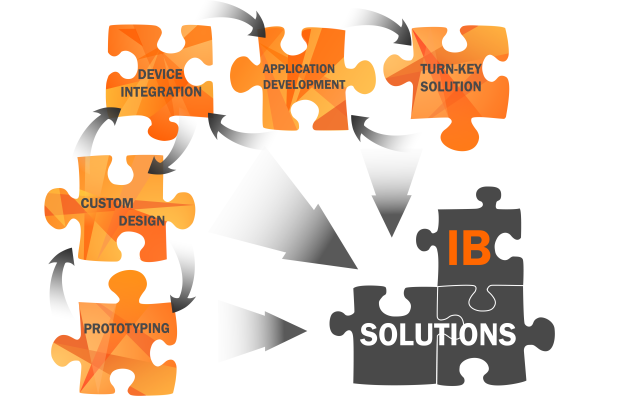
- Prototyping
- Custom Design
- Device Integration
- Application Development
- Testing
- Turn-key Solution
Experts in metrology, failure analysis, electron and ion optics, control and automation
Experienced team in successful delivery for leading global semiconductor companies for over 15 years
Coordinated with well-recognized advisors and collaborators world-wide
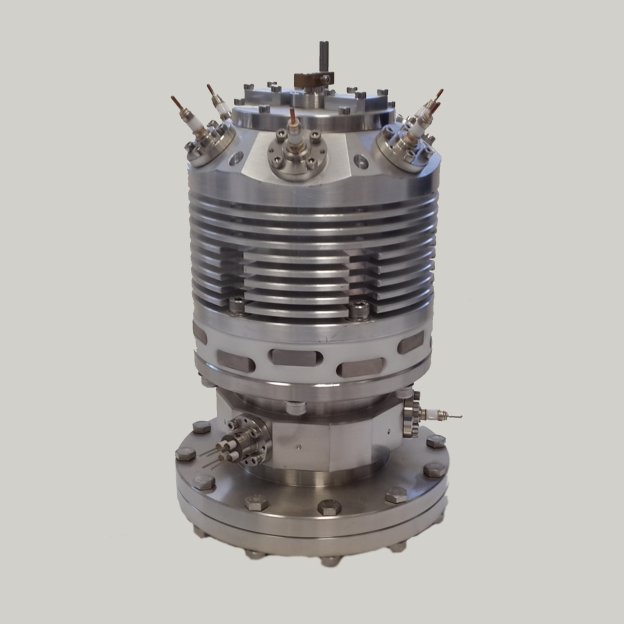
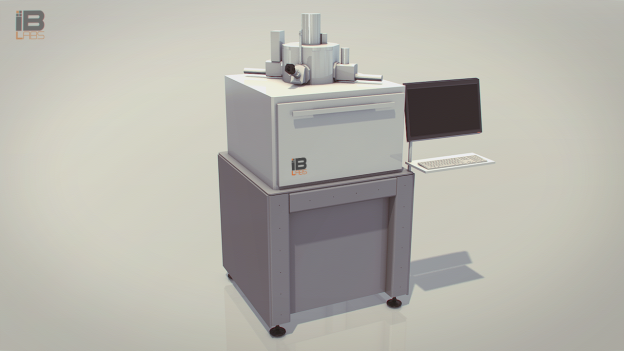
We design, manufacture and integrate equipment for nano-machining, imaging and failure analysis of integrated circuits and packages.
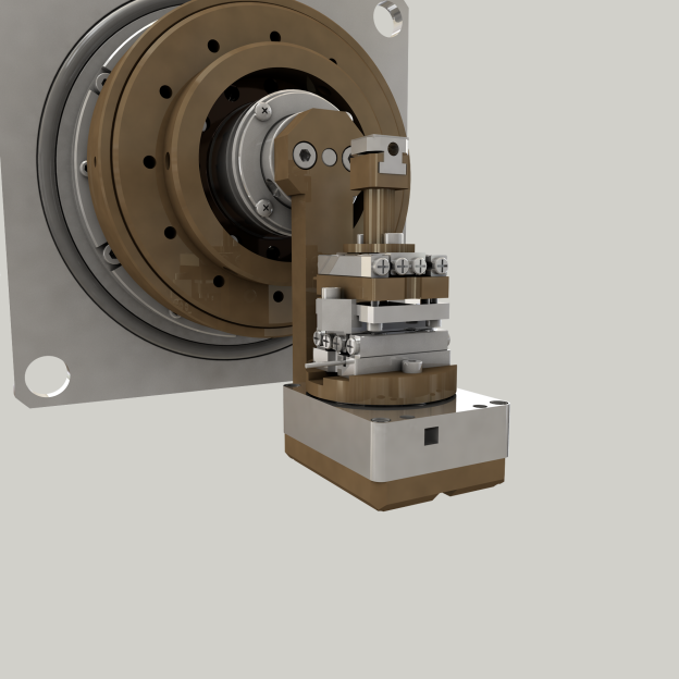
We enable 3D image reconstruction of structures of interest.
Our technology is compatible with a number of analytical techniques for materials analysis.