Welcome to IB Labs
We are a high-tech company in the field of metrology, nano machining and failure analysis of semiconductor devices. IB Labs introduces an entirely new concept of surface preparation for physical and electrical failure analysis and imaging.
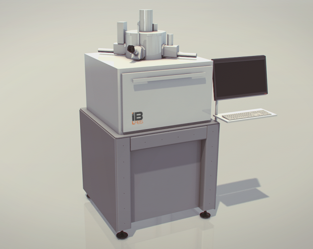
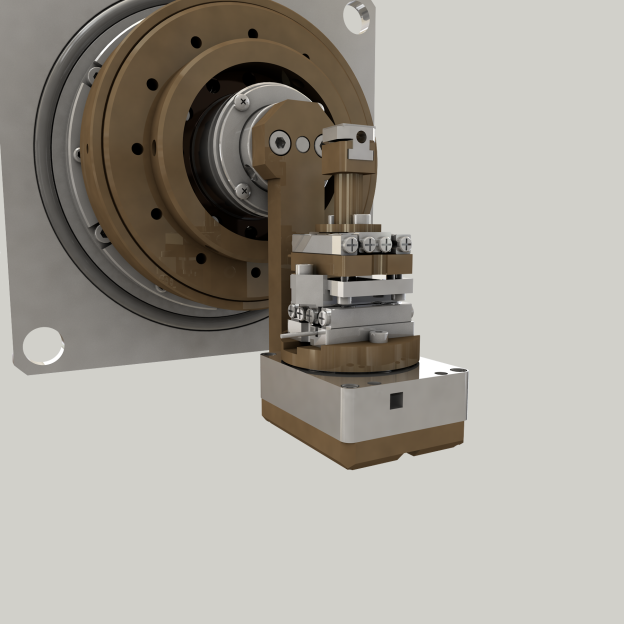
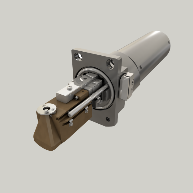
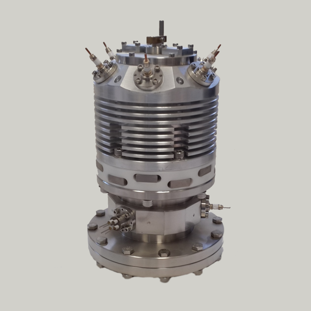
IB Labs’ solutions are based on its proprietary Universal Ion Beam (UIBTM) technology for site-specific in-situ ion-milling. Our technology uniquely combines maneuverable broad- and focused ion beams in a single tool, an Integrated Beam Unit (IBU). The IBU is a next-generation Surface Micro-machining tool for Yield Engineering and Failure Analysis. With its open-concept modular design, it is fully customizable. It is configurable as a stand-alone or integrated into existing Scanning Electron Microscopes, Mass- or Raman-spectrometers or other tools.
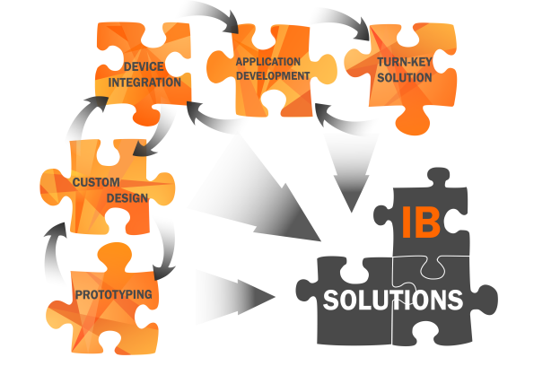
- Prototyping
- Custom Design
- Device Integration
- Application Development
- Testing
- Turn-key Solution
What we do
We design, manufacture and integrate equipment for nano-machining, imaging and failure analysis of integrated circuits and packages.
We enable 3D image reconstruction of structures of interest.
Our technology is compatible with a number of analytical techniques for materials analysis.
Why IB Labs
- Expertise
- Team of experts with proven track record to deliver in highly customer-centric environment
- Successful development and integration of state-of-the-art technologies and tools
- Intellectual Property (IP)
- Innovative development approach based on the company IP
- Best practices
- Good business and manufacturing practices proven at the leading hi-tech companies
Who we are
Experts in metrology, failure analysis, electron and ion optics, control and automation
Experienced team in successful delivery for leading global semiconductor companies for over 15 years
Coordinated with well-recognized advisors and collaborators world-wide
